
Knowledge
The Three Core Points of the Structure and Surface Requirements of Die-cast Parts

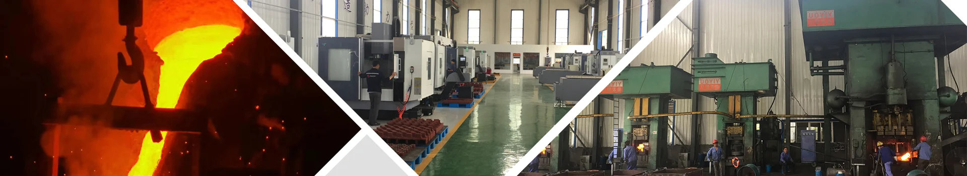
In fields such as new energy vehicles, consumer electronics, and industrial equipment, die-cast parts have become the main structural components due to their three major advantages: high production efficiency, integrated molding, and lightweight. However, many engineers often fall into a trap when designing - they only focus on strength and size, while neglecting surface quality. In fact, surface defects not only affect appearance but may also cause assembly jams, corrosion failures, and even functional abnormalities.
Based on the Vigor’s more than 20 years of die-cast part experience, this article dissects the surface requirements of die-cast part structural design from three dimensions: "casting mark control", "surface roughness matching", and "surface treatment adaptation", helping you avoid 90% of surface pitfalls!
I. Casting Marks: Hidden Minefields That Must Be Anticipated in Design
The casting marks on die-cast parts are the "process imprints" left by the metal liquid filling the mold. Some of these marks are visible to the naked eye (such as flash), while others are hidden at the microscopic level (such as microcracks), but all of them directly affect product quality. As structural designers, it is necessary to identify potential risk points in advance and clearly specify control requirements in the drawings.
1. Common Types of Casting Marks and Their Causes
Flash (Burrs): The most obvious "aesthetic killer", often appearing at parting lines and slider clearances. The causes are usually insufficient clamping force of the mold, poor fit of the parting line, or too small draft angle, which allows the metal liquid to squeeze into the clearance.
Flow marks / cold laps: The surface shows wavy or layered marks, resembling "unstirred milk tea". Essentially, it is caused by uneven filling speed of the molten metal (flow marks) or significant temperature difference between two metal streams (cold laps), commonly found near thin-walled corners or gates.
Shrinkage cavity / porosity: Small pits or microscopic pores visible to the naked eye, mostly distributed in thick and large areas (such as the end of the rib). It is mainly caused by insufficient feeding during the solidification and contraction of the molten metal. In structural design, "thick walls without support" is the main reason.
Scratches / Marks: Linear marks left on the casting due to damage on the mold surface, often occurring near the sliding core-pulling mechanism.
2. How to "proactively avoid pitfalls" during design?
Optimize structural features: Avoid sudden changes in wall thickness (it is recommended that the transition slope be ≥1:5), and add process holes or de-gating slots in thick areas (keep the thickness difference within 2:1).
Clarify draft requirements: All vertical surfaces must be designed with draft angles (≥1° for aluminum alloys and ≥0.5° for zinc alloys), and deep cavity structures should have additional "step draft".
Mark critical areas: On the drawings, use "dashed boxes + text" to indicate "flash ≤0.1mm" for parting lines and slider areas, and mark "no flow marks/cold shuts" for mating surfaces.
Integrate with process: Involve the die-casting factory in the design review to confirm the location of the parting line (avoid placing important appearance surfaces at the junction of the moving and fixed dies).
II. Surface roughness: It's not "the smoother, the better", but "customized as needed"
Surface roughness (Ra value) is a key indicator of the microscopic unevenness of the die-casting part's surface. Many novice engineers directly apply the roughness requirements for machined parts (such as Ra≤1.6μm), but the characteristics of the die-casting process mean that excessive pursuit of low roughness can increase costs and even cause defects.
1. The "natural boundary" of surface roughness for die-cast parts
The surface of die-cast parts is a "crystallization layer" formed by the rapid solidification of molten metal. Even if the mold is polished to Ra0.4μm, the actual surface roughness of the cast part can only reach Ra1.6-3.2μm (for aluminum alloys) or Ra0.8-1.6μm (for magnesium alloys). Forcing a reduction in roughness may require secondary machining (such as grinding or shot blasting), but this can damage the surface layer's density and reduce corrosion resistance.
2. Defining roughness by functional zones
Mating surfaces (such as bearing holes, bolt columns): Roughness should be controlled at Ra≤3.2μm (Ra≤1.6μm for critical fits), but sharp corners or deep grooves (which can trap burrs) should be avoided.
Appearance surfaces (such as consumer electronic casings): Customers typically require "no visible defects to the naked eye", which corresponds to Ra≤6.3μm, but flow marks and porosity should be controlled.
Non-mating/non-appearance surfaces (such as mounting back plates): Ra≤12.5μm is acceptable, but slight cold shuts or shrinkage porosity can be tolerated (the impact on strength needs to be evaluated).
3. "Roughness-friendly" design techniques
Avoid designing complex surfaces with "mirror finish" requirements (such as high-gloss chamfers on phone frames), as die-casting processes are difficult to achieve this.
For appearance surfaces, prefer "plane + shallow cavity" structures (depth ≤ 1/3 of wall thickness) to reduce flow mark accumulation.
Clearly mark on the drawings with "symbol + value":
For example, "Mating surface: Ra≤3.2μm (unmarked areas Ra≤6.3μm)".
III. Surface Treatment: Design should leave sufficient space for "post-processing"
Die-cast parts are rarely used as bare materials; most require surface treatment to enhance corrosion resistance, aesthetics, or functionality (such as conductivity). However, many designs ignore the limitations of the treatment process, resulting in parts that are "doable but difficult to do well", or even scrapping and rework.
Avoid closed structures: All deep cavities and blind holes should be designed with "process holes" (diameter ≥ φ3mm) for easy venting and drainage.
Reduce stress concentration: Avoid sharp corners and notches (R≥0.2mm) to prevent cracking during treatment (such as current concentration during electroplating).
Mark "untreatable areas": Use "diagonal fill + text" to indicate "no anodizing allowed in this area" (such as sensor mounting positions).
Synchronize with suppliers: Provide a "surface treatment flowchart" during design reviews to confirm the changes in key dimensions (such as hole diameter, wall thickness) after treatment (such as ±5μm for electroplating layer thickness).